In a major stride toward the future of high-speed data processing and photonics-electronics integration, Oki Electric Industry Co., Ltd. (OKI) has unveiled its proprietary Tiling Crystal Film Bonding (CFB) technology. This innovation addresses one of the most persistent challenges in semiconductor manufacturing: how to seamlessly integrate small optical semiconductor wafers onto large-scale silicon substrates.
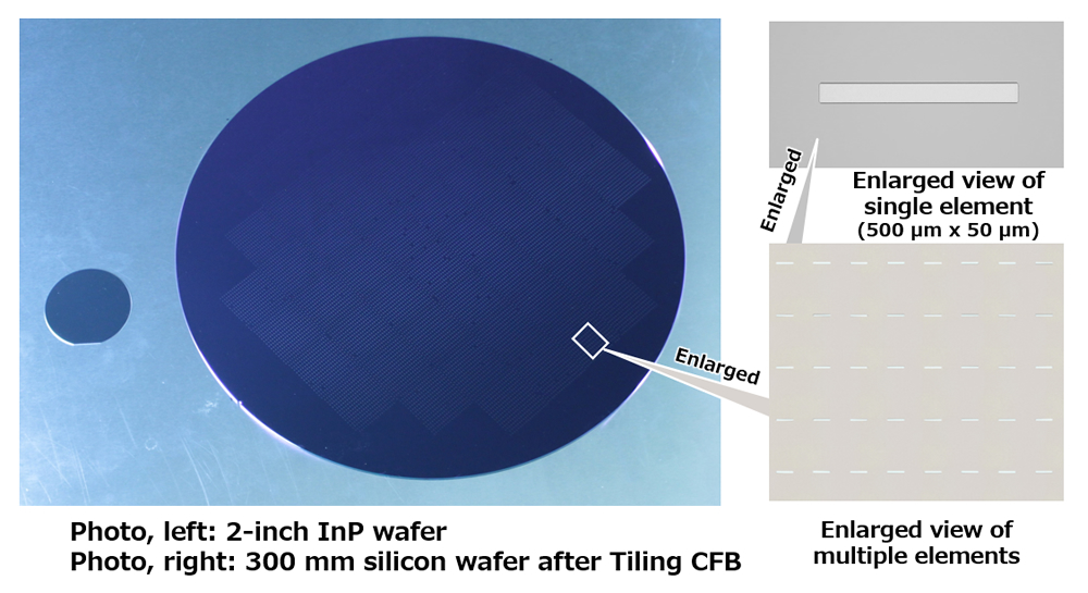
OKI’s Tiling CFB technique enables the precise placement of multiple small-diameter wafers, such as those made from indium phosphide (InP), onto a 300 mm silicon wafer—a standard size in advanced semiconductor fabrication. Key features of this technology include:
- Ultra-high alignment precision: ±1 μm in position and ±0.005° in rotation
- Adhesive-free bonding, preserving thermal and electrical conductivity
- Reusability of source wafers, reducing material waste
- Scalable tiling: Up to 52 transfers from a single 2-inch InP wafer
This method allows OKI to tile optical components like photonic waveguides across a large silicon platform without damaging delicate structures or compromising performance.
As demand surges for low-power, high-bandwidth data transmission—especially in AI, cloud computing, and data centers—the need for photonics-electronics convergence has become urgent. Traditional integration methods struggle with mismatched wafer sizes and incompatible materials. OKI’s solution elegantly sidesteps these issues, enabling:
- Hybrid chips that combine optical and electronic functions
- Energy-efficient interconnects for data centers
- Advanced AI processors with embedded photonic capabilities
Beyond technical prowess, Tiling CFB also supports eco-conscious manufacturing. By allowing the reuse of expensive InP wafers and eliminating adhesives, OKI reduces both cost and environmental impact—an increasingly vital consideration in semiconductor production.
OKI plans to collaborate with academic institutions and industry leaders to accelerate the commercialization of this technology. The goal? To usher in a new era of integrated photonic systems that are faster, smarter, and more sustainable.
Share to your social below!

The 55betlogin process was a breeze. No hassle, just straight to the games. Loving the easy access! Login Now 55betlogin
Hey, just found rummycirclenews.com. Seems like a decent place for rummy news and updates. I’ll be checking it out for strategies and stuff. rummycirclenews
Alright, checking out sara777rate.com. Hope they have honest reviews and ratings. Sick of all the biased stuff out there. Need some real opinions. sara777rate