The invisible world of precision requires special “ears.”
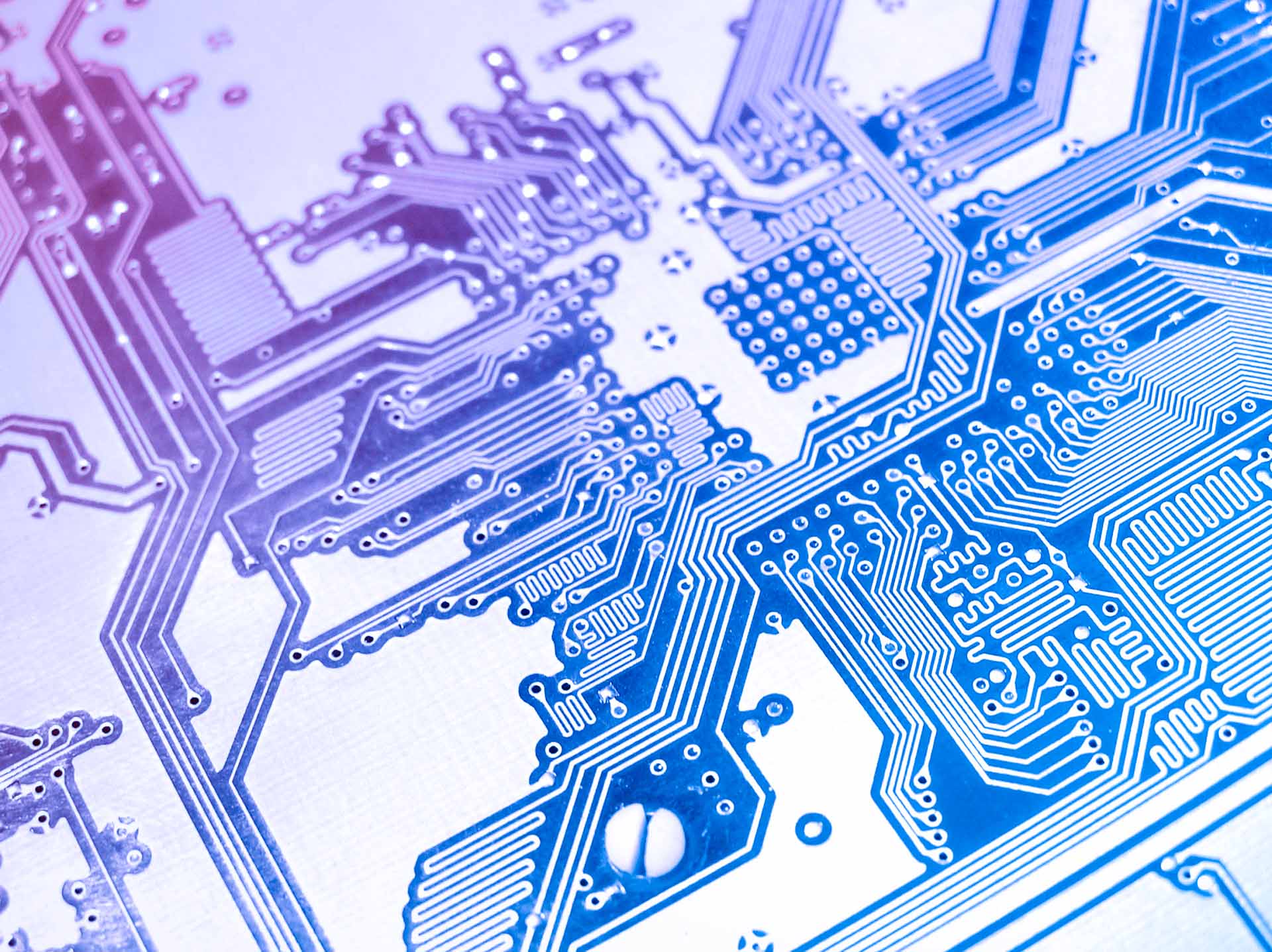
In modern technological products such as smartphones, computers, automotive electronics, and medical devices, chips serve as miniature “brains” and “hearts,” with internal structures that are far more intricate and complex than one might imagine. How can one examine the internal structure of a chip without damaging it? Ultrasonic testing technology provides engineers with a special “stethoscope,” making it an indispensable key technology for ensuring chip quality.
Basic principles of chip ultrasonic testing
Ultrasonic testing (UT) utilizes the propagation characteristics of high-frequency sound waves (typically exceeding 20 kHz) in materials to detect internal defects. When ultrasonic waves encounter discontinuities in the material (such as cracks, voids, or delamination), they produce reflections, refractions, or scatterings. By analyzing changes in these acoustic signals, the structural integrity of the material can be assessed.
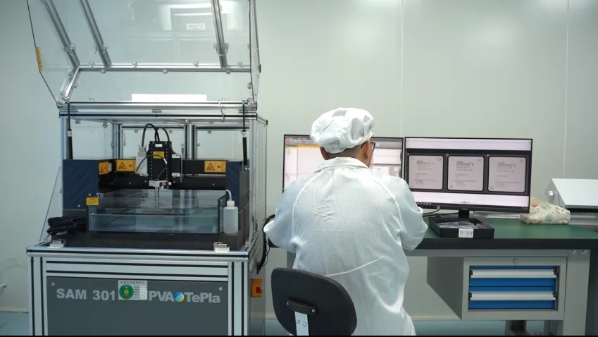
In chip inspection, ultrasonic frequencies can reach as high as 100 MHz to 2 GHz, far exceeding the 1 to 10 MHz commonly used in industrial ultrasonic testing. These high-frequency ultrasonic waves can detect defects as small as micrometers or even nanometers. The inspection process generally includes:
- The ultrasonic transmitter generates high-frequency pulses
- The sound waves are transmitted into the chip through a coupling medium
- The receiver captures the reflected sound wave signals
- The computer system processes the signals and generates an image
Why chips particularly need ultrasonic testing

The inevitable choice for non-destructive testing
The chip manufacturing process involves hundreds of steps and is extremely costly. Traditional destructive testing methods such as cross-section analysis are accurate but completely destroy the sample, limiting their use to sampling inspections. Ultrasonic testing enables 100% inspection without damaging the chip, which is particularly important for high-end processor chips worth thousands of dollars.
Challenges in detecting multi-layer structures
Modern chips use three-dimensional stacking technology and may contain dozens of interconnected structures. X-ray inspection is not sensitive to defects parallel to the beam direction, while ultrasonic waves are particularly sensitive to interface layering defects and can effectively detect quality issues in critical areas such as bonding interfaces and micro-bump connections.
The “nemesis” of packaging defects
Statistics show that approximately 30% of chip failures are caused by the packaging process rather than the silicon wafer itself. Ultrasound can accurately detect the following packaging defects:
- Voids and cracks in the plastic encapsulation material
- Delamination between the chip and the substrate
- Poor connection between solder balls and bumps
- Lead bonding quality issues
The critical role of ultrasonic testing in the chip lifecycle

research and development phase
- Verify the reliability of new packaging designs
- Evaluate the compatibility of different material combinations
- Optimize process parameters
production phase
- Real-time monitoring of bonding process quality
- Detection of early manufacturing defects
- Prevention of defective products from entering downstream processes
Reliability testing phase
- Evaluate interface degradation after temperature cycling
- Detect material delamination caused by moisture penetration
- Predict product life
Failure analysis phase
- Quickly locate the fault point
- Avoid destroying critical evidence
- Provide scientific evidence required for litigation
The silent guardians on the quality front line
While people enjoy the convenience brought by electronic technology, few realize the critical role that ultrasonic testing technology plays in this process. It serves as the “stethoscope” of the electronics industry, quietly safeguarding the internal integrity of every chip. As China’s semiconductor industry continues to rise, developing domestically controlled, high-end ultrasonic testing equipment and technology is of great significance for ensuring the security of the industrial chain. In the future, smarter and more precise ultrasonic testing technology will continue to safeguard chip innovation, becoming an indispensable guardian of electronic product quality.
Share to your social below!