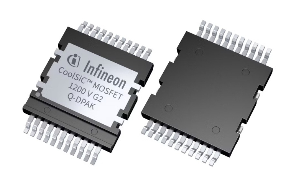
Infineon Technologies has announced the launch of its next-generation CoolSiC™ MOSFET 1200 V G2, housed in a top-side-cooled (TSC) Q-DPAK package. This innovation marks a significant leap in thermal performance, system efficiency, and design flexibility for demanding industrial applications such as EV chargers, solar inverters, motor drives, and solid-state circuit breakers.
The CoolSiC 1200 V G2 introduces several enhancements over its predecessor:
- Up to 25% lower switching losses for equivalent R_DS(on) values
- 15% reduction in thermal resistance
- 11% lower MOSFET operating temperature
- Supports overload operation up to 200°C junction temperature
These improvements are enabled by Infineon’s advanced .XT die attach interconnection technology, which enhances heat dissipation and reliability under dynamic conditions.
The Q-DPAK package is engineered for top-side cooling, allowing direct heat transfer from the device’s surface to the heatsink. This design:
- Improves heat transfer efficiency compared to bottom-side cooling
- Minimizes parasitic inductance for higher switching speeds
- Supports compact system layouts
- Is compatible with automated assembly for scalable manufacturing
Infineon offers the CoolSiC 1200 V G2 in two configurations:
- Single switch
- Dual half-bridge
Both are part of the broader X-DPAK platform, which features a standardized 2.3 mm package height across TSC variants (including Q-DPAK and TOLT). This allows engineers to mix and match components under a single heatsink, simplifying system design and scaling.
The CoolSiC MOSFET 1200 V G2 is tailored for:
- Electric vehicle (EV) chargers
- Solar inverters
- Uninterruptible power supplies (UPS)
- Motor drives
- Solid-state circuit breakers
Its broad R_DS(on) range (4 mΩ to 78 mΩ) gives designers the flexibility to optimize performance across various power levels and operating conditions.ality.
Share to your social below!

References:
Manoir de beauregard https://nanniedenh506016.amoblog.com/casino-of-gold-dein-ultimativer-guide-63656892
References:
Rainbow casino wendover ricetteclara.com